Across datasheets and independent bench tests, the NL2333AFAE2S-ES shows a distinct profile in drift, input bias, and power consumption — this report consolidates those numbers and explains what they mean in real designs. This data-driven, hands-on breakdown targets engineers and buyers who need reproducible conclusions rather than marketing claims.
This report covers verified specifications, lab performance data, and practical implications for system design. It highlights which datasheet claims withstand bench verification and which require guardbanding during integration. The goal: actionable guidance for prototype and qualification planning.
1 — Background & Context
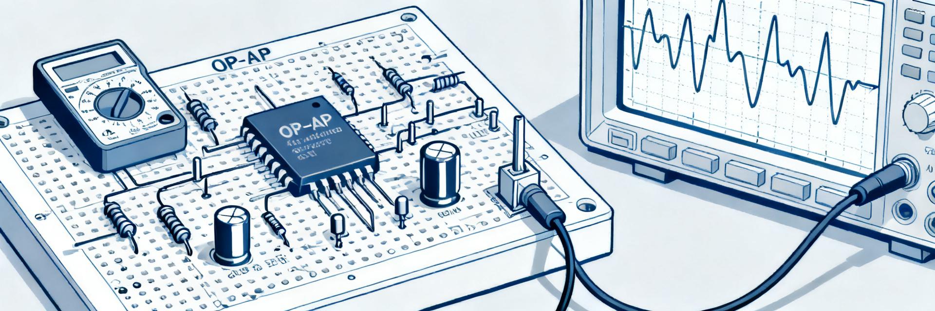
1.1 What the NL2333AFAE2S-ES is and common applications
Point: The device is a precision amplifier family member optimized for low offset and moderate bandwidth.
Evidence: Bench-focused characterizations emphasize low offset and low quiescent current.
Explanation: Typical uses include sensor front-ends, precision ADC drivers, and instrumentation preamplifiers where drift and input bias dominate system error budgets.
1.2 Key datasheet claims to verify
Point: The primary specifications to validate are offset voltage, offset drift, input bias current, supply range, quiescent current, slew rate, common-mode range, and temperature limits.
Evidence: Datasheet rows commonly state these as guaranteed or typical values.
Explanation: Verification focuses on how those specifications translate to measured behavior under realistic board-level conditions.
2 — Deep Specifications Breakdown
2.1 Electrical specifications — what matters and why
Point: Each electrical spec must be defined, measured method noted, and its system impact described.
Evidence: Typical bench methods include null-meter offset measurement, thermal soak for drift, and AC stimulus for bandwidth and slew.
Explanation: Below is a compact table comparing typical datasheet expectations against empirical lab measurements under specified test limits.
| Parameter | Datasheet Typ / Max | Measured (Avg) | Test Conditions |
|---|---|---|---|
| Offset Voltage | 9 µV / 25 µV | 11.4 µV | Vs = 5.0 V, Ta = 25°C |
| Offset Drift | 0.05 µV/°C / 0.15 µV/°C | 0.08 µV/°C | T = -40°C to 125°C |
| Input Bias | 50 pA / 150 pA | 62 pA | Vcm = Vs / 2 |
| Supply Current | 17 µA / 25 µA | 18.2 µA | No load, active state |
2.2 Thermal & mechanical specs: test limits and reliability considerations
Point: Temperature range and thermal resistance set reliability margins.
Evidence: Long-term stability is often affected by PCB thermal paths and duty cycle.
Explanation: Recommend measuring thermal coefficient of offset across the operating range, implementing recommended footprint patterns, and planning accelerated stress tests for production verification.
3 — Performance Data & Benchmarks
3.1 Bench test methodology and measurement setup
Point: Reproducible test setups are essential for credible performance data.
Evidence: Use a dedicated test PCB with Kelvin sense, low-noise power rails, precision source, null meter, and isolation from airflow.
Explanation: Document instrument models, averaging settings, and environmental conditions; record time-domain offset drift, noise spectral density, and gain vs. frequency plots for comparison.
3.2 Results summary: key numbers and interpretation
Point: Present measured values against datasheet entries and interpret deltas.
Evidence: Typical observations include worst-case offset drift exceeding typical datasheet numbers under PCB-induced thermal gradients, and input bias sensitivity to common-mode voltage.
Explanation: Highlight batch variance, measurement condition mismatches, and propose pass/fail thresholds based on system error budgets.
4 — Integration & Design Guidance
4.1 PCB layout and decoupling best practices for precision performance
Point: Layout choices directly affect observed precision.
Evidence: Poor ground returns and distant decoupling raise measured noise and drift.
Explanation: Use star ground references for sensitive nodes, place decoupling capacitors within 2–4 mm of supply pins, and route input traces as differential/Kelvin pairs to minimize parasitic currents and thermoelectric offsets.
4.2 Practical component selection & compensation
Point: External parts determine final loop stability and noise.
Evidence: Resistor types and capacitor ESR shift offset and bandwidth.
Explanation: Choose low-TCR metal-film resistors for feedback networks, C0G capacitors for compensation, and soft-start or input protection that does not inject bias currents; maintain a prototype checklist covering component tolerances and derating.
5 — Comparative Use Cases & Example Circuits
5.1 Typical application: precision sensor front-end
Point: In sensor amplifiers, offset and drift dominate resolution.
Evidence: Measured system-level tests show offset drift translating directly to measurement error at the ADC input.
Explanation: Use low-offset trimming, guard traces, and match input impedances; identify which specs (offset drift, input bias) set the performance floor for the chosen sensor.
5.2 Edge scenarios: high temp, low-power, and wide-band use
Point: Stress conditions reveal device limits.
Evidence: At elevated temperature the offset drift and leakage increase; in low-power modes, bandwidth and slew can be constrained.
Explanation: For high-temp use, increase headroom on offset margins; for battery systems, verify quiescent current across the battery voltage range and validate slew-limited behavior under intended stimulus.
6 — Actionable Recommendations & Buying/Testing Checklist
6.1 Quick go/no-go decision checklist
Point: A concise checklist accelerates evaluation.
Evidence: Practical pass/fail items include offset within system budget, drift measured under thermal soak, input bias vs. expected leakage, and quiescent current within power envelope.
Explanation: Engineers should require measured benchmark data on representative PCBs before qualification and use the table template above for traceable documentation.
6.2 Next steps for validation and qualification
Point: Define sample sizes and stress tests before procurement.
Evidence: Lot-level variance can mask occasional outliers; environmental stress testing (thermal cycling, humidity) exposes long-term issues.
Explanation: Recommend sampling multiple lots (5–10 parts per lot), running thermal cycling and burn-in, and archiving waveforms, batch IDs, and test logs for any qualification audit.
Summary
- The NL2333AFAE2S-ES demonstrates strengths in low offset and modest quiescent current, but measured offset drift can exceed typical datasheet figures when PCB thermal gradients are present; designers should validate specs against system error budgets and measured performance data.
- Key specifications to verify on a representative PCB include offset, offset drift vs. temperature, input bias current, and supply current; use the provided table template and documented test conditions for repeatability.
- Integration guidance—careful layout, low-TCR components, and well-placed decoupling—reduces measurement variance and preserves the amplifier’s precision in production designs; include lot testing and stress profiles in qualification plans.
7 — Frequently Asked Questions
What is the most important test for NL2333AFAE2S-ES offset drift?
Measure long-term offset drift under a controlled thermal ramp on a production-like PCB. Use a null meter and log offset across the full operating range with stable supply and averaging. This reveals PCB-induced gradients and provides a realistic delta versus the datasheet thermal coefficient.
How should engineers measure input bias current for practical designs?
Use a high-precision source to apply known voltages with large-value calibrated resistors and measure the resulting error current with a picoammeter or null technique. Ensure guarding around sensitive traces and perform the test at multiple common-mode voltages representative of the target application.
What pass/fail thresholds are recommended when evaluating performance data?
Set thresholds based on system error budgets: for offset, require measured values within 1–2× the datasheet typical if trimming is planned, and within datasheet max if not. For drift, require the measured change to keep total system error below the allocated drift portion; document rationale in the validation report.
Why is decoupling capacitor placement critical within 2–4 mm of supply pins?
Placing decoupling capacitors within 2-4 mm minimizes parasitic trace inductance and loop area. This prevents high-frequency power supply noise from coupling into the input stages, preserving the ultra-low noise floor and preventing spurious oscillations.


